Etching Process which you are looking for are available for all of you here. we have 29 examples about Etching Process including images, pictures, models, photos, etc. In this article, we also have variation of pictures usable. Such as png, jpg, animated gifs, pic art, logo, black and white, transparent, etc about Etching Process.
Not only Etching Process, you could also find another pics such as Oil Seal, Stainless Steel, Aluminum, Chemical, Dry, Printmaking, Art, Acid, Mold, Bosch, PCB, and Anisotropic.
.jpg) 1920 x 800 · jpeg chemical etching process etching information from www.masteretching.com
1920 x 800 · jpeg chemical etching process etching information from www.masteretching.com 1200 x 897 · png pv manufacturingorg from pv-manufacturing.org
 820 x 344 · png learn display etching from global.samsungdisplay.com
 1000 x 700 · png chemical etching process step step precision micro from www.precisionmicro.com
 577 x 950 · png photo etching find suppliers processes material from www.manufacturingguide.com
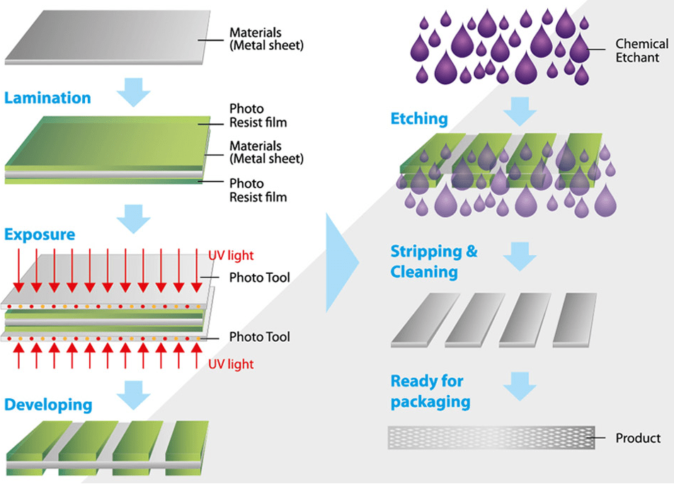
 0 x 0 chemical etching process chemical etching from www.masteretching.com
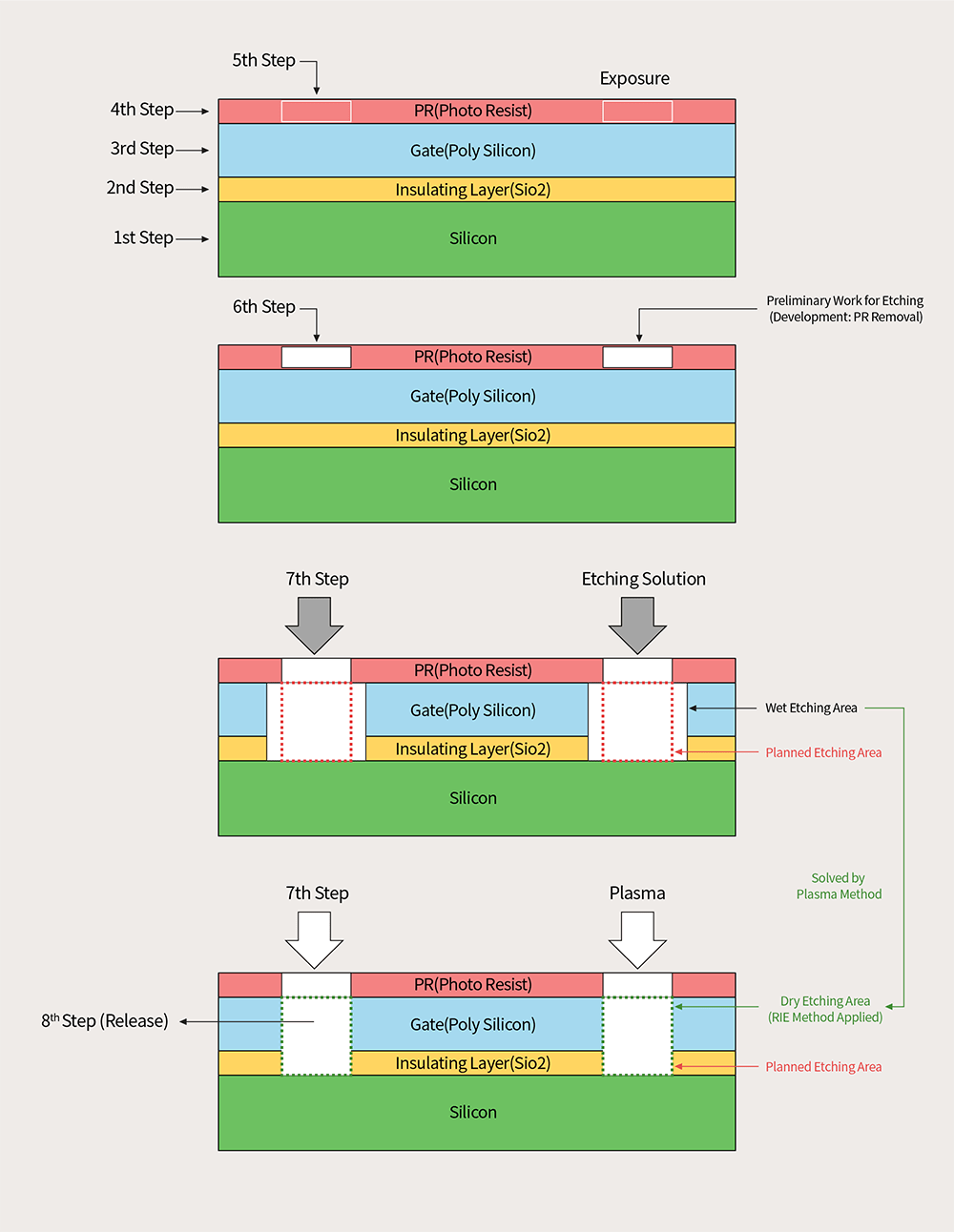 1000 x 1292 · png etching process complete semiconductor patterning sk hynix newsroom from news.skhynix.com
952 x 684 · png tecford design pcm from www.tecforddesign.com
1000 x 1292 · png etching process complete semiconductor patterning sk hynix newsroom from news.skhynix.com
952 x 684 · png tecford design pcm from www.tecforddesign.com 2560 x 1707 · jpeg photo etching process step step guide uwe from www.uweinc.com
 670 x 418 · jpeg chemical etching photo etching processsinoguide specialist photo etching china from www.sg-etch.com
 695 x 501 · jpeg effect etching process vlsi concepts from www.vlsi-expert.com
 1920 x 1280 · jpeg chemical etching process step step guide garden sport outdoor tools from www.lflus.com
 1568 x 1045 · jpeg types stainless steel etching process hysonetch from www.hysonetch.com
 1920 x 1080 · jpeg acid etching acid types metal types applications benefits from www.iqsdirectory.com
 1600 x 837 · jpeg chemical etching companies chemical etching services from www.metaletching.org
 474 x 316 · jpeg arkansas metal etching from www.metaletching.org
 1600 x 900 · jpeg stainless steel etching companies services from www.metaletching.org
 920 x 670 · jpeg acid etching precision process business advice guide from www.business-advice-guide.com
 1334 x 1334 · jpeg photo chemical etching process advanced metal etching from metaletching.com
 1024 x 768 · jpeg etching process design talk from design.udlvirtual.edu.pe
 1879 x 1780 · jpeg plasma surface etching henniker plasma treatment from plasmatreatment.co.uk
 1024 x 768 · jpeg etching process from www.slideshare.net
 1024 x 664 · jpeg chemical etching metal fabrication processes from metaletching.com
 475 x 557 · png etching materials research institute from www.mri.psu.edu
 1200 x 800 · jpeg chemical etching process kecheng from kcetching.com
 527 x 535 · gif surface finishing tutorial technical tutorial misumi from www.misumi-techcentral.com
 1296 x 1080 · jpeg acid etching steps pictures instructables from www.instructables.com
 620 x 413 · jpeg pcb etching process steps video allpcb from www.allpcb.com
 1000 x 1000 · jpeg step step guide etching pcbs from www.wellpcb.com
Don't forget to bookmark Etching Process using Ctrl + D (PC) or Command + D (macos). If you are using mobile phone, you could also use menu drawer from browser. Whether it's Windows, Mac, iOs or Android, you will be able to download the images using download button.


